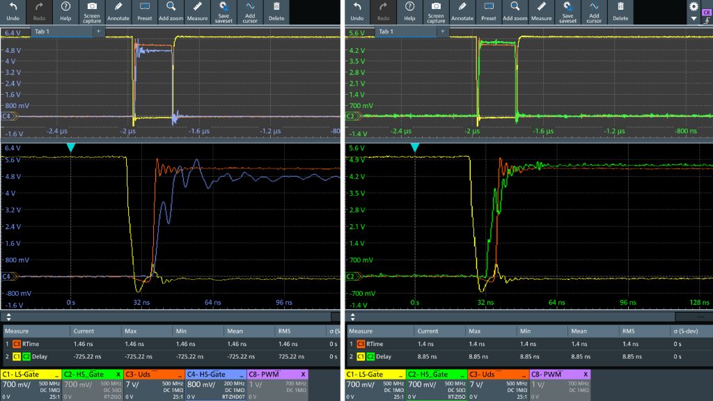
Common mode distortion of wide-bandgap power electronics probing

In an ideal scenario, a probe accurately transmits a signal from the device under test (DUT) in its original form with no alterations. Differential probes are designed to eliminate common-mode (CM) distortion by cancelling out identical signal artifacts on each socket relative to earth. In practice, issues such as poor CM rejection, frequency response degradation and signal distortion can compromise signal integrity, particularly in high-speed power applications where signal fidelity is crucial.

Your task

When working on fast switching power semiconductors such as wide-bandgap (WBG) devices, fast and high voltage (HV) swings are common. The rise/fall time of devices such as those made from gallium nitride (GaN) have a range of < 2 ns, which require a higher bandwidth probing solution of up to 1 GHz. To optimize signal integrity in such power applications, probe setup performance and frequency response need to minimize distortion and signal degradation.

HV differential probes are often used to measure signals without a ground reference in a high-side gate source voltage for a half-bridge converter. Note here the commonmode rejection ratio (CMRR) of these probes especially at high frequencies help suppress fast environmental CM noise.

FET setup
FET setup
Open Lightbox

Limitation of conventional HV differential probe

A common misconception is that standard differential probes are fully earth isolated across their entire bandwidth. In reality, the differential amplifier in these probes is earth referenced, creating a return path for CM signals when used with a measurement instrument and inherently limiting their CMRR performance. While 4 mm banana plug cables have HV ratings necessary for power measurements, they lack controlled impedance and proper shielding, especially at higher frequencies. Hence, conventional HV differential probes typically provide bandwidths of up to 400 MHz with limited CM noise suppression of about –20 dB. For every 10 V of CM signals, 1 V appears as noise in measurements.

Isolated power conversion design
Open Lightbox

Breaking the CM ground loop

To effectively measure WBG power devices, which operate at higher voltages and faster switching speeds, full galvanic isolation between the DUT and the measuring device is essential to limiting the CM return path and reducing noise. One popular approach for isolation is inductive or opto-coupling used in isolated-channel oscilloscopes.

However, long and unshielded cables can still introduce noise along the signal path. The distance of the probe from the DUT’s measurement point must be minimized. Replacing traditional probes tips with coaxial tips can help maintain proper impedance matching and improve measurement accuracy.

R&S®RT-ZISO isolated probing system
Open Lightbox

Rohde & Schwarz solution

R&S®RT-ZISO isolated probing system:

  • Bandwidth: 100 MHz to approximately 1 GHz
  • Input range: ±3540 V (RMS)
  • CM range: ±60 kV
  • CMRR at 1 GHz: 90 dB
  • Highest sensitivity: ±10 mV range

The R&S®RT-ZISO isolated probing system is designed with this measurement approach in mind. The probe head connects to the DUT over a short coax probe tip (MMCX) to shield the measured signals from CM noise and maintain stable and matching impedance, letting the probe operate even at high frequencies of up to 1 GHz. The probe head converts the measured signals into optical signals and transmits them to the receiver box, breaking the CM ground loop and reducing disturbance during the measurement.

Probe tip CMRR performance and input voltage derating over frequency
Open Lightbox

When characterizing high-side WBG gate-source input, the switch node (C3) applies fast switching CM voltage to the measurement point. The high-side gate voltage (C4, screenshot below, left side) is highly affected by the CM noise when using conventional HV differential probes.

The R&S®RT-ZISO captures the same gate voltage (C2, screenshot below, right side) with slightly faster edges and less noise. The noise seen on HV differential probes (C4) has a huge perturbation and takes longer to settle down. Waveform details of gate voltage where the Miller plateau and charging time could be of interest can be highly disturbed and concealed by CM noise.

Summary

The R&S®RT-ZISO isolated probing system minimizes the impact of high-frequency CM noise in WBG power measurements, so that CMRR performance meets expectations across the operating frequency range. The probe tip connector type can impact overall CMRR, so include testing requirements when designing a product for optimal measurement results.

Comparison of the HS gate measurement between conventional HV differential probes and the isolated probing systems shows more details hidden by the CM noise manifest in a conventional system